On January 11, 2026, engineers and scientists from the Lawrence Livermore National Laboratory (LLNL) collaborated with Stanford University to develop a groundbreaking 3D nano-manufacturing method. This new approach transforms two-photon lithography (TPL) technology from a slow, lab-scale technique into a wafer-scale manufacturing tool, all while maintaining sub-micron precision.
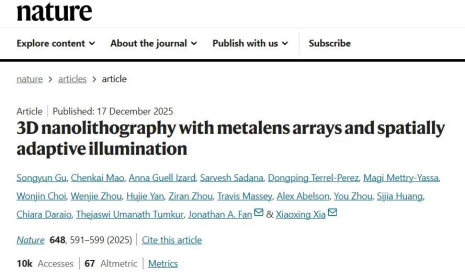
The research team’s findings were published in Nature magazine under the title “3D nanolithography with metalens arrays and spatially adaptive illumination.”
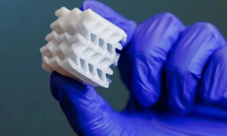
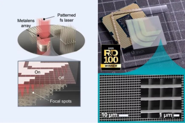
This work utilizes large, ultra-thin optical component arrays—metasurface arrays—to split a femtosecond laser into over 120,000 collaboratively focused spots that can simultaneously write over a centimeter-scale area. This metasurface-based approach enables the creation of complex 3D structures with a minimum feature size of 113 nanometers, achieving throughput that is over a thousand times faster than commercial systems.
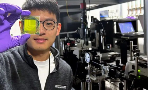
Xiaoxing Xia, a materials engineer and lead researcher at Lawrence Livermore National Laboratory (LLNL), said, “When this 3D printing system first achieved precision at one and three centimeters, seeing our concept, developed over three to four years, finally come to life was truly astonishing. Seeing the printing speed hundreds or even thousands of times faster than our commercial printers, and with such high precision, we realized that this technology had made a breakthrough.”
From Niche Laboratory Technology to Scalable Manufacturing
For many years, TPL technology has been favored for its nanoscale resolution, but due to its reliance on microscope objectives, the printable area was limited to a few hundred micrometers. Printing larger areas required stitching together thousands of tiles, a slow process that introduced alignment errors and hindered TPL technology from leaving the laboratory.
The research team’s metasurface dual-photon laser scanning (TPL) method replaces the microscope objective with a set of high numerical aperture metasurface arrays, with each metasurface acting like a micro-sized printer. The new TPL system does not scan a single beam of light but instead prints thousands of small regions in parallel, with all regions seamlessly fused in a single scan. By setting the focus distance to the spacing of the metasurfaces, rather than squeezing them into a tiny light field, this system avoids the proximity effects that plagued earlier multi-beam methods.
The first author of the paper, a postdoctoral researcher at Lawrence Livermore National Laboratory (LLNL), stated: “This means that TPL finally has the potential for industrial application. Previously, it was purely a research tool. With advancements in wafer-level nano-manufacturing technology, we hope to manufacture nanomaterials and micro-devices just like we make computer chips. While computer chips are highly complex, they are mass-produced at a very low unit cost. Metasurface optics is the solution to this problem.”
Adaptive Light Control Unlocks New Design Freedom
To print non-periodic structures, the research team integrated a spatial light modulator that can adjust the intensity of each focal point in real-time. The modulator can switch beams on and off, adjust the line width through grayscale control, and arrange the beams layer by layer to form larger patterns. Originally designed to balance beam intensity, this approach unexpectedly unlocked broader design freedom.
Professor Xia said: “During the project, we discovered that by dynamically switching the focal points and carefully planning the printing paths, we could print completely random structures in a highly parallel manner. Gu and Savish (collaborators) printed 16 different microscopic chess openings in a single print session. To thank the advanced manufacturing lab at Lawrence Livermore National Laboratory for their tremendous support, the research team named this method Adaptive Metasurface Lithography Technology.”
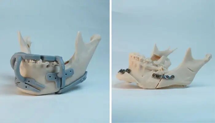
This parallel and adaptive approach enables metasurface dual-photon laser technology to manufacture a wide variety of products, from gradient density laser targets and flexible terahertz devices to millions of micro-particles daily. It can also create complex modular architectures for emerging technologies in microfluidics, quantum information, microelectronics, photonics, fusion energy, and biomedicine. What excites researchers the most is that this technology holds the potential to advance transformative R&D projects at LLNL, such as 3D printing fusion fuel capsules and trapping ion quantum computing chips.
Professor Xia believes that the integration of optics and additive manufacturing is a decisive step in the development of additive technologies. He stated, “Light is the finest chisel on Earth, capable of creating functional materials and microstructures. New ways of controlling light will completely change the way materials are manufactured.”
With the development of higher power lasers, larger metasurface wafer sizes, and faster modulators, the research team believes that metasurface dual-photon laser printing (TPL) technology will be able to print more complex devices at higher speeds, driving 3D nano-manufacturing technology toward mainstream wafer-level production. This technology platform, named MetaLitho3D, recently won the 2025 R&D 100 Award, demonstrating its potential for widespread adoption in the industry and its ability to solve real-world problems.